DC Power supply
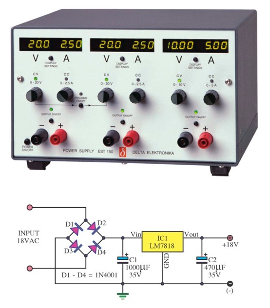
Almost all electronic devices used in electronic circuits need a DC source of power to operate.
For portable low power systems Batteries may be used, but their operating period is limited. For Long term operation frequent recharging and replacement of Batteries become much costlier and complicated.
In practice, D.C. power for electronic circuits is most conveniently obtained from commercial A.C. lines by using rectifier-filter system, called a ordinary d.c. power supply, also called as Unregulated D.C. power supply.
Power supply: A group of circuits that convert the standard ac voltage (240 V, 50 Hz) provided by the wall outlet to constant dc voltage.

Unregulated D.C.Power Supply
A group of circuits used to convert ac to dc.
- Rectifier – Converts ac to pulsating dc.
- Filter – Reduces variations in the rectifier output.
Limitations:
- The d.c. output voltage changes directly with input a.c. voltage.
- The d.c. output voltage decreases as the load current increases.
Regulated D.C.Power Supply
A group of circuits used to convert ac to dc.
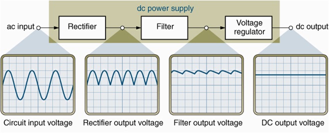
- Rectifier – Converts ac to pulsating dc.
- Filter – Reduces variations in the rectifier output.
- Voltage regulator – Maintains a constant dc output voltage.
Transformers
Although not a popular design, some power supply circuits are transformer less . Direct rectification of AC line power is a viable option in some applications :
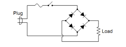
Transformers is used to step-up or step-down (usually to step-down) the supply voltages as per the need of solid state electronic devices and circuits to be supplied by the dc power supply.
It can provide isolation from the supply line – an important safety consideration. The issue of isolation is a safety concern.
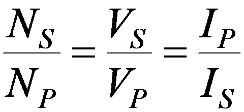
Transformers are described in terms of the relationship between secondary voltage (VS) and primary voltage (VP).
- Step-up – VS is greater than VP.
- Step-down – VS is less than VP.
- Isolation – VS is approximately equal to VP.

Transformer Voltage and Current Ratios
Diode
A diode is a device that passes current in only one direction.
It is a bit like a water-valve that prevents water back-flowing into the mains from your property. or a valve in a pump that prevents the water flowing back down a well.
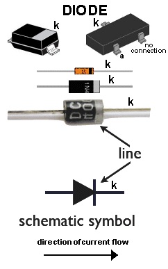
A diode has two leads. These are called ANODE and CATHODE.

The cathode end is identified in a circuit diagram and on the body of the device.
It may be identified with a line, dimple or a symbol. There must be something on the diode that identifies this lead and you have to look for it.
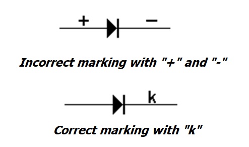
A diode does NOT have a positive or negative end. You see this mistake in so many discussions. A diode will have a positive voltage on the anode and a slightly lower (positive) voltage on the cathode. It will not have a positive on the anode and negative on the cathode.
Important Terms
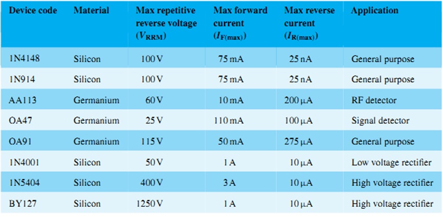
(i)Forward current: It is the current flowing through a forward biased diode. Every diode has a maximum value of forward current which it can safely carry. If this value is exceeded, the diode may be destroyed due to excessive heat. For this reason, the manufacturers data sheet specifies the maximum forward current that a diode can handle safely.
(ii) Peak inverse voltage: It is the maximum reverse voltage that a diode can withstand with- out destroying the junction. If the reverse voltage across a diode exceeds this value, the reverse current increases sharply and breaks down the junction due to excessive heat. Peak inverse voltage is extremely important when diode is used as a rectifier.
(iii)Reverse current or leakage current: It is the current that flows through a reverse biased diode. This current is due to the minority carriers. Under normal operating voltages, the reverse current is quite small. Its value is extremely small (< 1 µA) for silicon diodes but it is appreciable (100 µA) for germanium diodes.
Characteristics of some typical signal and rectifier diodes
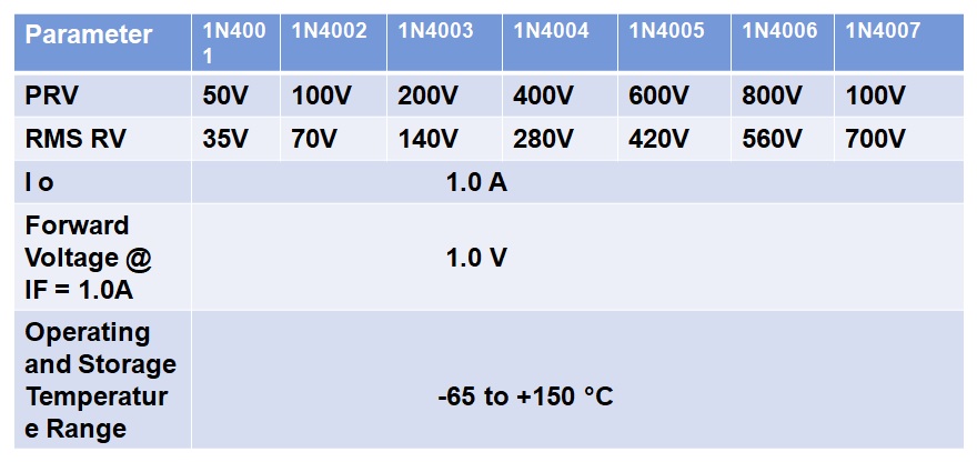
Characteristics of 4000 series diodes
Diode Applications
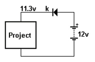
The diode as a protection diode
In the following diagram, the diode does not conduct if the battery is connected around the wrong way. It is called a PROTECTION DIODE. This means the circuit will not see a reverse voltage and will not be damaged. However the circuit will see a voltage 0.7v less than the voltage of the battery due to the 0.7v drop (lost) across the diode.
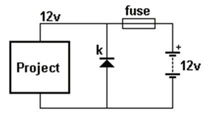
In the following circuit, the diode conducts if the battery is connected around the wrong way and creates a SHORT-CIRCUIT. This will burn-out the fuse. The diode is called a PROTECTION DIODE.
Using a diode as a voltage reference
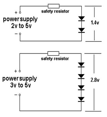
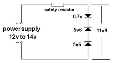
Other applications
- Clippers
- Clampers
- Logic Gates
- Rectifiers
Rectifiers
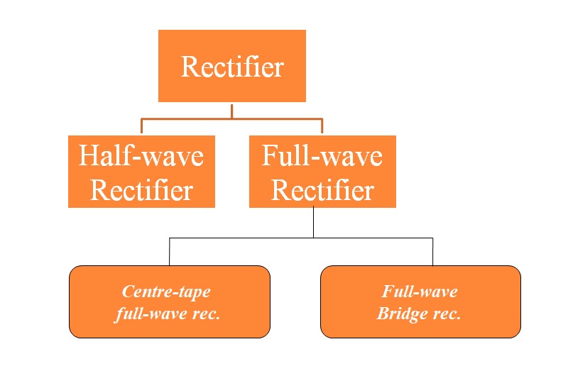
Half-wave Rectifiers
Half-wave rectifier – A diode placed in series between a transformer (or ac line input) and its load.
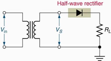
Positive Half-wave Rectifiers
This circuit converts an ac input to a series of positive pulses.
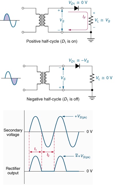
Average Load Voltage and Current
Average voltage (Vave) – The dc equivalent of a voltage waveform.
Average current (Iave) – The dc equivalent of a current waveform.
For the output from a half-wave rectifier:

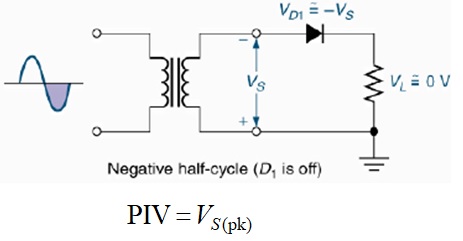
Peak inverse voltage (PIV) – The maximum diode reverse bias produced by a given circuit.
For the diode in a half-wave rectifier:
Advantages :
Simple circuit and low cost.
Disadvantages :
The main disadvantages of a half-wave rectifier are :
(i) The pulsating current in the load contains alternating component whose basic frequency is equal to the supply frequency. Therefore, an elaborate filtering is required to produce steady direct current.
(ii) The a.c. supply delivers power only half the time. Therefore, the output is low and rectifier efficiency is low (40.6%)
Find D.C output voltage?
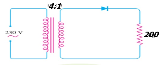
R.M.S secondary voltage = 230(N2/N1) =230(1/4) = 57.5V
Max. voltage across secondary (Vm) = 57.5 x √ 2 = 81.3 V
Idc = Vm/ ∏ RL =0.13A
Vdc = Idc x RL = 0.13 x 200 = 26V
(OR)
Vdc = Vm/ ∏ = 81.3/3.14 = 26V
Full-wave Rectifier
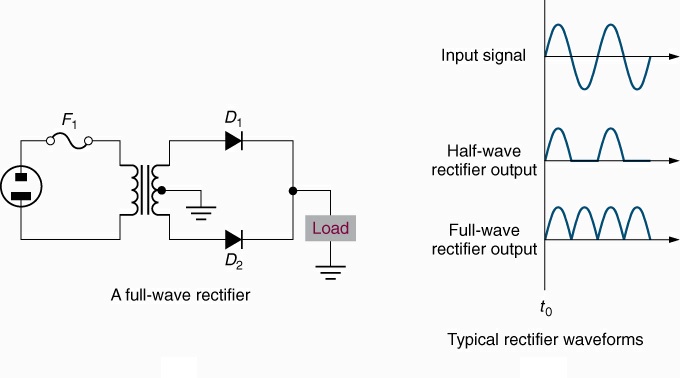
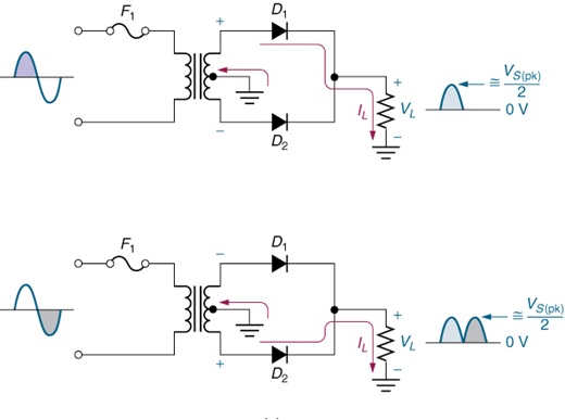
Diodes conduct during alternate half cycles of the input signal.
VL(pk) is approximately half the value of VS(pk).
The circuit produces two positive half-cycles for each input cycle.
Average Load Voltage and Current
Average voltage (Vave) – The dc equivalent of a voltage waveform.
Average current (Iave) – The dc equivalent of a current waveform.
For the output from a full-wave rectifier:

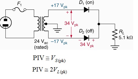
Peak Inverse Voltage (PIV)
Peak inverse voltage (PIV) – The maximum diode reverse bias produced by a given circuit.
PIV For the diode in a full-wave rectifier:
Find D.C output voltage?
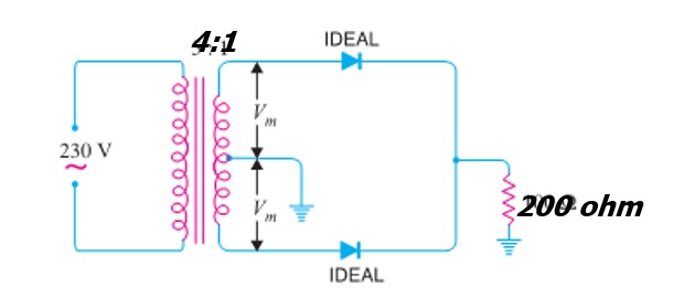
R.M.S secondary voltage = 230(N2/N1) =230(1/4) = 57.5V
Max. voltage across secondary = 57.5 x √ 2 = 81.3 V
Max. voltage across half secondary (Vm) = 81.3/2 = 40.65 V
Idc = 2 Vm/ ∏ RL =0.129A
Vdc = Idc x RL = 0.129 x 200 = 25.9V
(OR)
Vdc = 2Vm/ ∏ = 81.3/3.14 = 25.9V
Full-Wave Bridge Rectifiers
The most commonly used because:
- It does not require the use of a center-tapped transformer.
- It can be coupled directly to the ac power line.
- It produces a higher dc output than a comparable full-wave center-tapped rectifier.
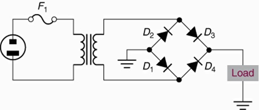
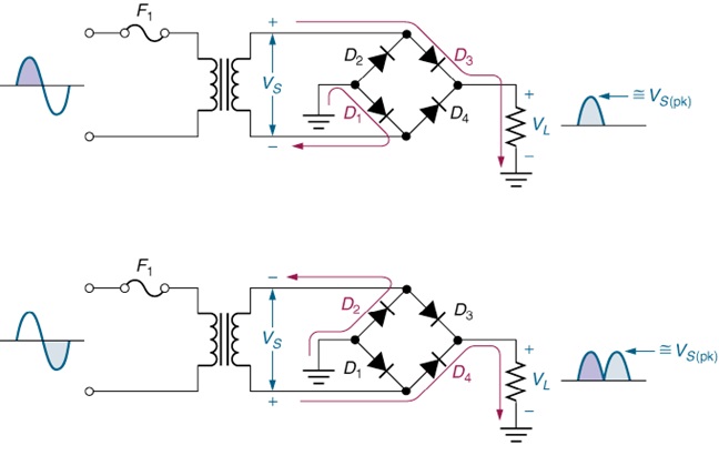
Bridge Rectifier Operation
Conduction alternates between two diode pairs.
Calculating load voltage and current relationships
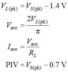
Find D.C output voltage?

R.M.S secondary voltage = 230(N2/N1) =230(1/4) = 57.5V
Max. voltage across secondary (Vm) = 57.5 x √ 2 = 81.3 V
Idc = 2 Vm/ ∏ RL =0.26A
Vdc = Idc x RL = 0.26 x 200 = 52V
(OR)
Vdc = 2Vm/ ∏ = 126.6/3.14 = 52V
Working with Rectifiers
Rectifiers are high current circuits, so IFRB can have a significant impact on diode forward voltage (VF ).
Cooling is often used to minimize the effects of high power rectifier reverse current. Components may be cooled using a fan and/or a heat sink.
High transformer tolerances can introduce significant discrepancies between calculated and measured current and voltage values.
Integrated Rectifiers
Integrated Rectifier – A rectifier circuit that is etched on a single piece of silicon (housed in a single case).
IC rectifiers are:
Cheaper to produce
Easier to troubleshoot
The diodes in an IC rectifier operate at the same temperature, so they have equal values of forward voltage and leakage current. IC rectifier cases are designed to be attached easily to a heat sink.
COMPARISON OF RECTIFIERS
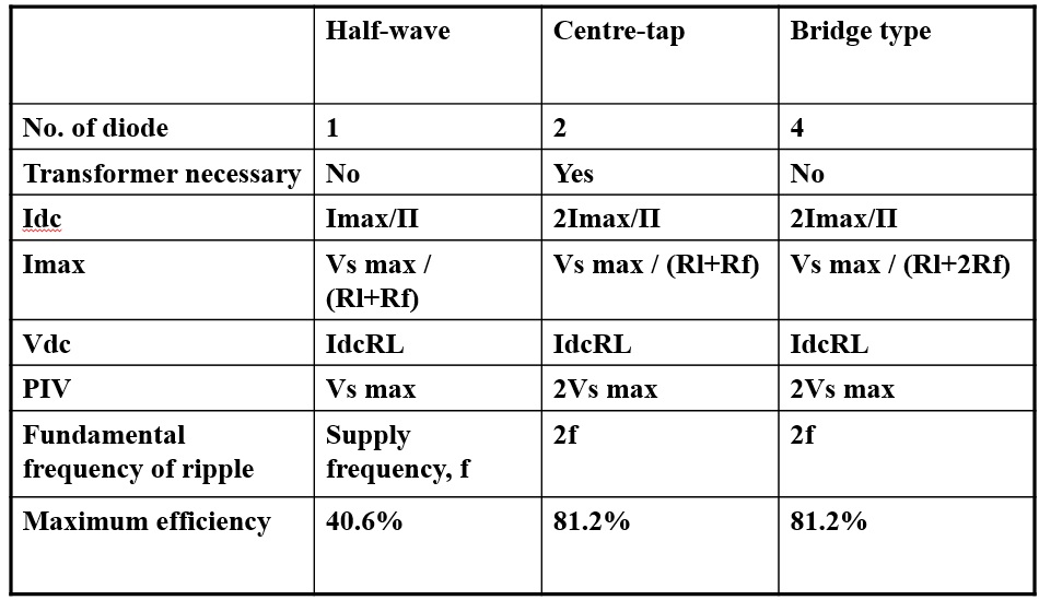
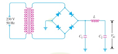
Filter circuit
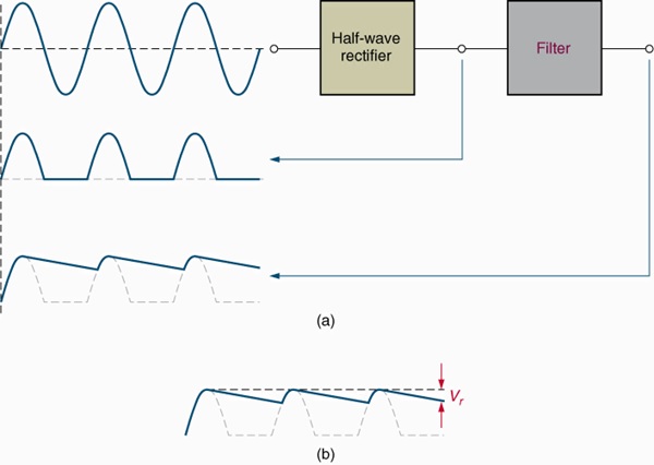
A filter circuit reduces the voltage and current variations in the output from a rectifier.
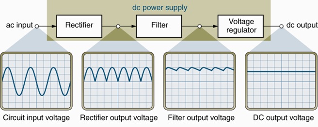
Ripple Voltage (Vr)
Ripple voltage (Vr) – The variation in the filter output voltage.
Voltage Regulators
Voltage regulator –A circuit used to produces a constant dc output voltage by reducing the ripple to negligible amount.
DC power supply final circuit:

Zener diode
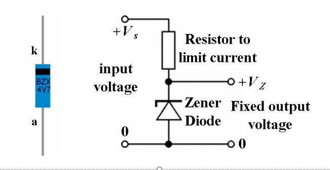
A Zener diode is a PN junction that has been specially made to have a reverse voltage Breakdown at a specific voltage.
Its characteristics are otherwise very similar to common diodes.
In breakdown the voltage across the Zener diode is close to constant over a wide range of currents thus making It useful as a shuntvoltageregulator.
Zener Voltage Regulators
For low current power supplies - a simple voltage regulator can be made with a resistor and a zener diode connected in reverse.
Zener diodes are rated by their breakdown voltage Vz and maximum power Pz (typically 400mW or 1.3W)
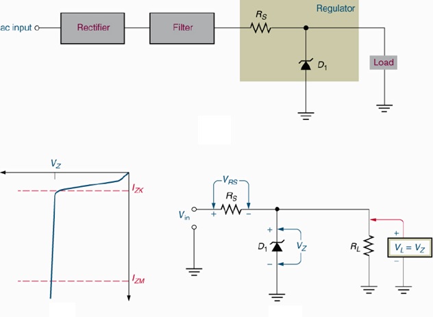
A Basic DC Power Supply

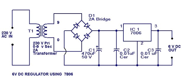
DC Power Supply using regulator
Power Supply Characteristics

DC Power Supply using regulator

Power Supply Characteristics
Load Regulation - The load regulation or load effect is the change in regulated output voltage when the load current changes from minimum to maximum value.
% Load Regulation = [(Vno-load - Vfull-load)/Vfull-load] * 100
The smaller the load regulation, the better the power supply. A well-regulated power supply can have a load regulation of less than 1% (i.e., the load voltage varies less than 1% over the full range of load current).
Source/Line Regulation - The source regulation is defined as the change in regulated output voltage for a specified rage of line voltage.
% Line Regulation = [(V hl – V ll)/V hl] * 100
The smaller the line regulation, the better the power supply. A well-regulated power supply can have a line regulation of less than 0.1
Minimum Load Resistance - The load resistance at which a power supply delivers its full-load rated current at rated voltage is referred to as minimum load resistance.
Minimum Load Resistance = Vfull-load/Ifull-load
Ripple Factor: The ratio of r.m.s. value of a.c. component to the d.c. component in the rectifier output is known as ripple factor.
Ripple Factor = V ac (rms) / V dc
Ripple factor is very important in deciding the effectiveness of a rectifier. The smaller the ripple factor, the lesser the effective a.c. component and hence more effective is the rectifier.
A power supply A delivers 10 V dc with a ripple of 0.5 V r.m.s. while the power supply B delivers 25 V dc with a ripple of 1 mV r.m.s. Which is better power supply ?
For power supply A, Ripple Factor = 5%
For power supply b, Ripple Factor = 0.004%
Clearly, power supply B is better.
Types of Regulator
The fundamental classes of voltage regulators are linear regulator and switching regulators.
Two basics types of linear regulator are :
Series Regulator
Shunt Regulator
Linear Power supply:
By sampling a portion of the output voltage and comparing it to a fixed reference voltage , the series pass element is used in the form of "variable resistor" to control and regulate the out put voltage.Series pass transistor operates in Linear region.
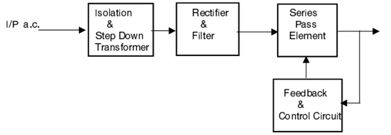
Basic Linear Series Regulator
In series regulation the control element is in series with the input and output.
Simple series voltage regulator and block diagram
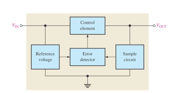
Basic op-amp series regulator
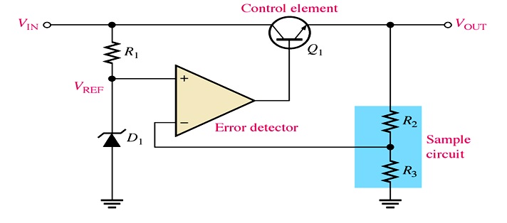
The control element is a transistor in series with the load.
The output sample circuit senses a change in the output voltage.
The error detector compares the sample voltage with a reference voltage (zener diode)
Control is achieved by controlling the voltage across Q1.
Regulating Action
The resistive voltage divider formed by R2 and R3 senses any changes in the output voltage.
When the output voltage tries to decrease, a proportional voltage decrease is applied to the op-amp’s inverting input by the voltage divider.
Zener diode sets the reference voltage for the non-inverting input of the op-amp. Any changes in the output are fed back to the inverting input of the op-amp.
The difference voltage (error voltage) is amplified and the op-amp’s output voltage is increased.
This increase is applied to the base of Q1 – causing the emitter voltage to increase until the voltage to the inverting input equals the reference voltage.
The regulated output voltage of the series regulator is:

Short-Circuit or Overload Protection
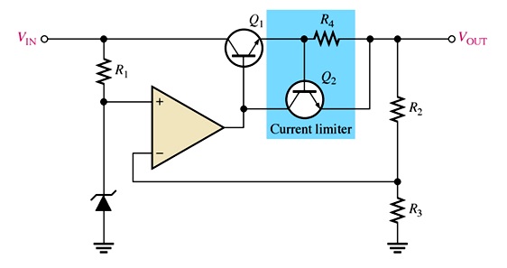
Overload protection for a series regulator protects the control element in the case of a short. Also known as constant-current limiting.
The load current through R4 produces a voltage from base to emitter of Q2.
When IL reaches a predetermined maximum value, the voltage drop across R4 is sufficient to forward – biased the base – emitter junction of Q2 – causing it to conduct.
When load current exceeds the predetermined level, Q2 diverts current from the base of Q1- reducing the load current through Q1 – preventing any additional of load current.
Basic Linear Shunt Regulator
In shunt regulation the control element is in parallel with input and output.
Simple shunt voltage regulator and block diagram
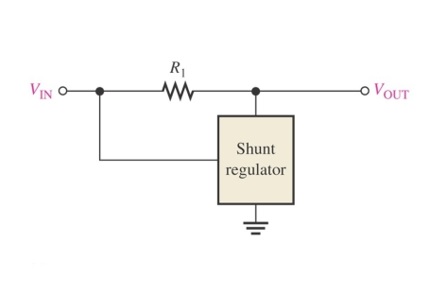
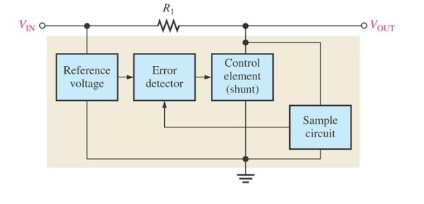
Basic op-amp shunt regulator with load resistor
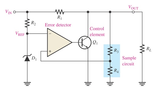
The control element is a transistor, Q1 parallel (shunt) with the load and a resistor R1 in series with the load.
The operation same as series, except that regulation is achieved by controlling the current through Q1.
Regulating Action
When the output voltage tries to decrease due to a change in input voltage or load current, the attempted decrease is sense by R3 and R4 - applied to the op-amp’s non-inverting input.
The difference voltage increases the op-amp’s output voltage - - and increasing the collector voltage, Vc – keeping the output nearly constant.
A shunt voltage regulator has the following drawbacks:
(i)A large portion of the total current through Series resistor (R1) flows through transistor rather than to the load.
(ii) There is considerable power loss in Series resistor (R1).
(iii) There are problems of overvoltage protection in this circuit.
For these reasons, a series voltage regulator is preferred over the shunt voltage regulator.Linear Power supply - Limitations:
The input transformer is bulkey and the most expensive component of the linear regulated power supply mainly because of low line frequency (50 Hz)
Because of low line frequency, large values of filter capacitors are required to decrease the ripple.
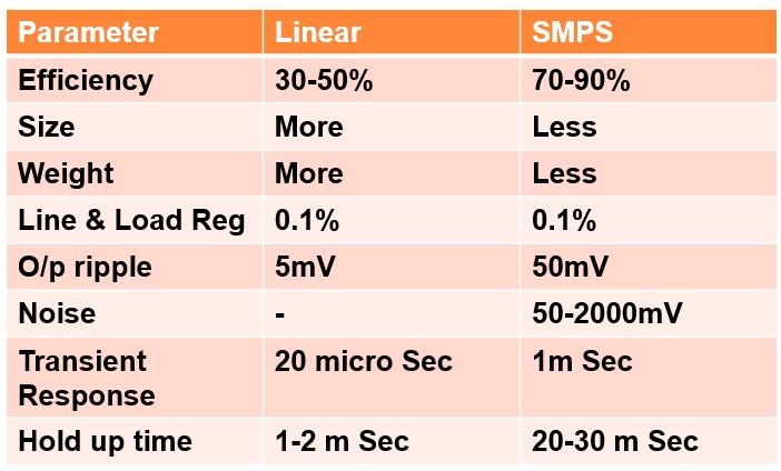
The series pass transistor operates in active region, it dissipates a lot of power as heat, necessitating use of heavy heat sinks & resulting in low efficiency between 30-50%
The input voltage must be greater than the output voltage. The Greater the difference in I/P & O/P more will be the power dissipated.
Switching Regulator
The switching regulator is more efficient, small size and low cost than the linear series or shunt type.
Greater efficiency achieved since the pass devise is operated as a low impedance switch (cutoff/saturation)
This type regulator is ideal for high current applications since less power is dissipated.
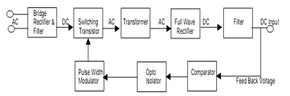
Basically, a switching regulator passes voltage to the load pulses, which are then filtered to provide a smooth dc voltage.
With switching regulators 70-90% efficiencies can be achieved.
High operating frequency – smaller capacitors , transformers and inductors (decrease in size and cost)
Basic Block diagram of SMPS
Limitations & Precautions
Since the rectifier is tied directly to the ac line voltage, the rectifier, capacitors and switching transistors must be able to withstand the peak line voltage (310V for 220 V ac rms line)
It is slow in responding to transient load changes compared to the conventional series regulator.
One should be more careful about the electromagnetic and radio frequency interference while using SMPS.
A SMPS is more complex and requires external components like inductors and transformers.
Difference between Linear and SMPS
IC Voltage Regulators
Regulation circuits in integrated circuit form are widely used.
Their operation is no different but they are treated as a single device with associated components.
These are generally three terminal devices that provide a positive or negative output.
Some types have variable voltage outputs.
A typical 7800 series voltage regulator is used for positive voltages.
The 7900 series are negative voltage regulators.
These voltage regulators when used with heatsinks can safely produce current values of 1A and greater.
The capacitors act as line filtration.
Fixed Voltage Regulator
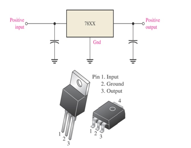
The fixed voltage regulator has an unregulated dc input voltage Vi applied to one input terminal, a regulated output dc voltage Vo from a second terminal, and the third terminal connected to ground.
Fixed-Positive Voltage Regulator
The series 78XX regulators the three-terminal devices that provide a fixed positive output voltage.
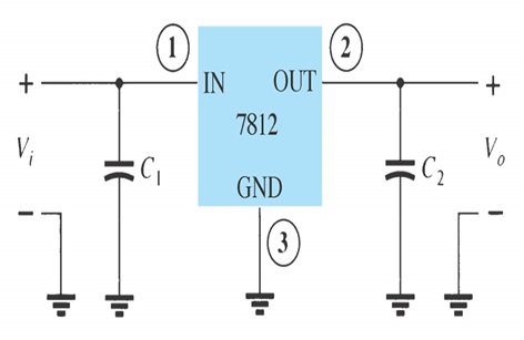
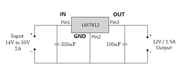
An unregulated input voltage Vi is filtered by a capacitor C1 and connected to the IC’s IN terminal.
The IC’s OUT terminal provides a regulated +12 V, which is filtered by capacitor C2.
The third IC terminal is connected to ground (GND)
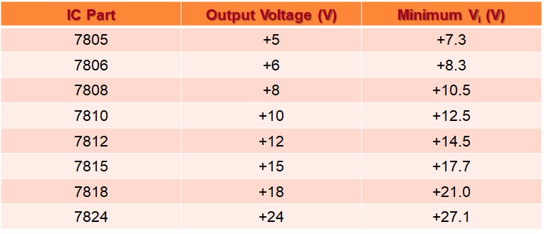
Seven O/P options in 78 XX series : 5,6,8,12,15,18 and 24V
Two extra voltage options in 79 XX series : -2V and -5.2V
Positive-Voltage Regulators in the 78XX Series
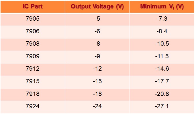
Fixed-Negative Voltage Regulator
The series 79XX regulators are the three-terminal IC regulators that provide a fixed negative output voltage.
This series has the same features and characteristics as the series 78XX regulators

Negative-Voltage Regulators in the 79XX Series
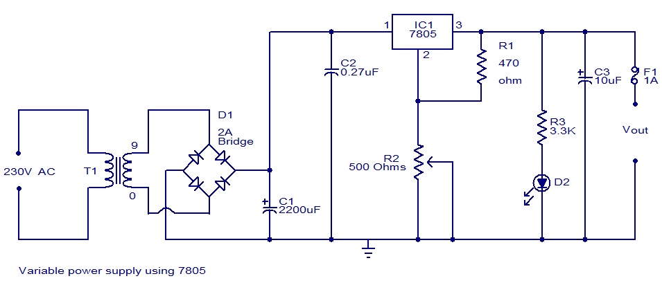
Variable PS using Fixed Regulator
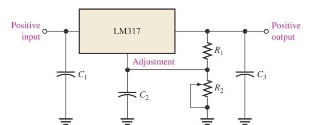
Adjustable-Voltage Regulator
Voltage regulators are also available in circuit configurations that allow to set the output voltage to a desired regulated value.
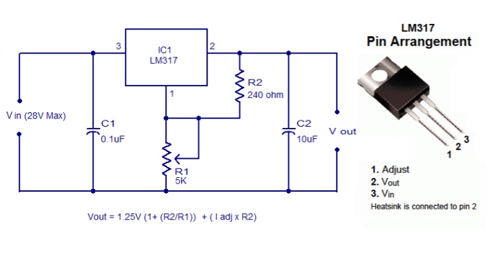
The LM317 is an example of an adjustable-voltage regulator, can be operated over the range of voltage from 1.2 to 37V.
LM150/LM350A/LM350 3-Amp Adjustable Regulators.
LM 138/338 3-Amp Adjustable Regulators.
Power Supply Circuits
5V regulator using 7805
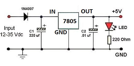
12V DC power supply using 7805
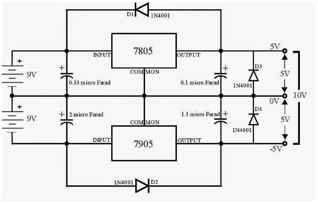
+5V/-5V DC power supply using 7805 and 7905
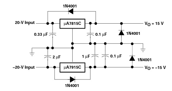
+15V/-15V DC power supply using 7815 and 7915
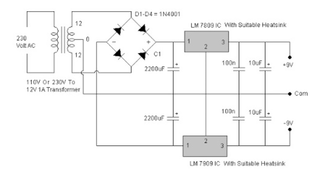
+9V/-9V DC power supply using 7809 and 7909
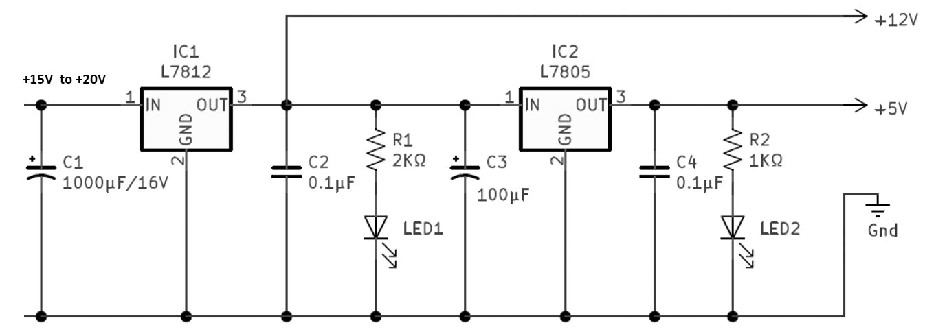
+12V,+5V DC power supply using 7812 and 7805
Variable Voltage output using LM317
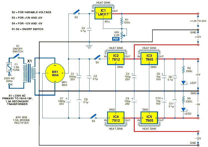
+/- 12 V, +/- 5V FIXED AND +1.25 to 20V VARIABLE POWER SUPPLY
